- 您现在的位置:买卖IC网 > Sheet目录3879 > PIC18F4539-E/PT (Microchip Technology)IC PIC MCU FLASH 12KX16 44TQFP
2002 Microchip Technology Inc.
Preliminary
DS30485A-page 197
PIC18FXX39
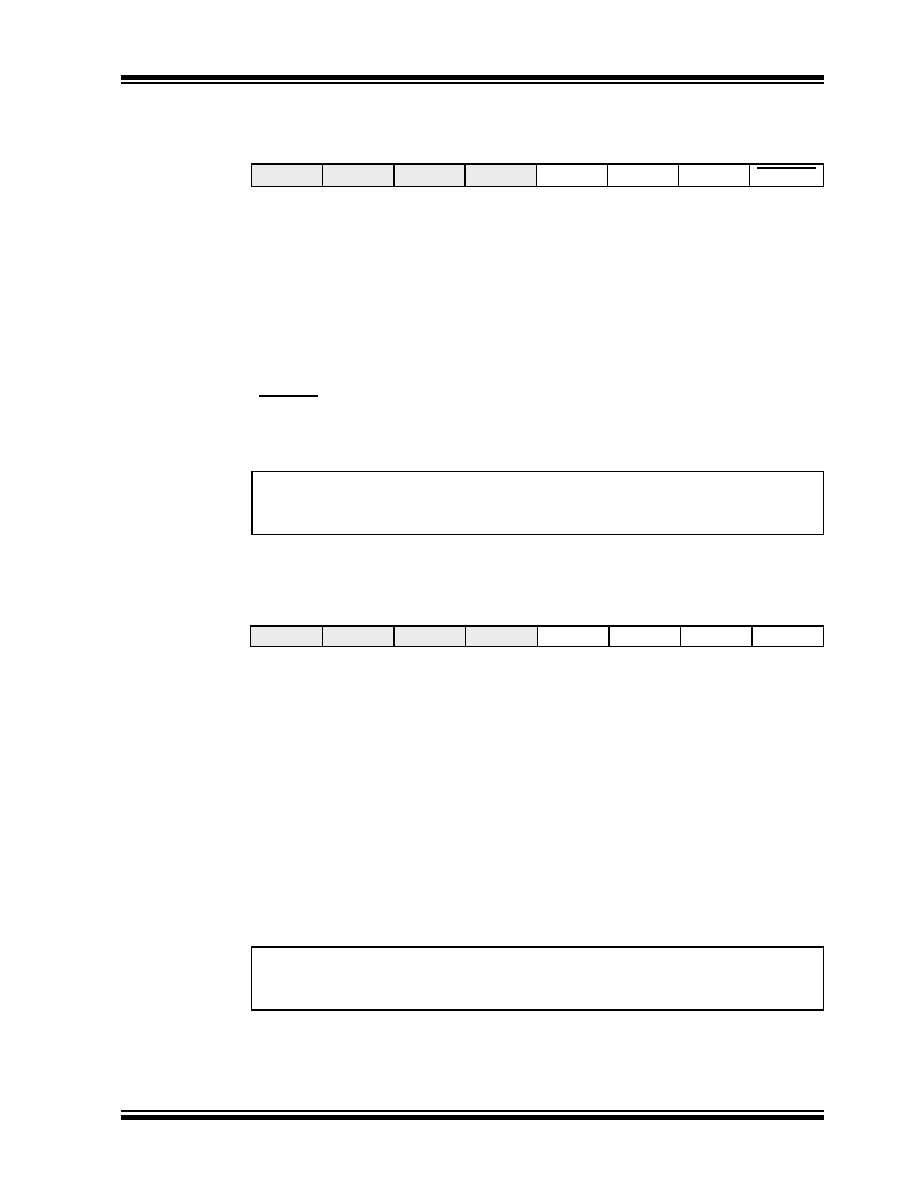
REGISTER 20-2:
CONFIG2L: CONFIGURATION REGISTER 2 LOW (BYTE ADDRESS 300002h)
REGISTER 20-3:
CONFIG2H: CONFIGURATION REGISTER 2 HIGH (BYTE ADDRESS 300003h)
U-0
R/P-1
—
BORV1
BORV0
BOREN
PWRTEN
bit 7
bit 0
bit 7-4
Unimplemented: Read as ‘0’
bit 3-2
BORV1:BORV0: Brown-out Reset Voltage bits
11
= VBOR set to 2.5V
10
= VBOR set to 2.7V
01
= VBOR set to 4.2V
00
= VBOR set to 4.5V
bit 1
BOREN: Brown-out Reset Enable bit
1
= Brown-out Reset enabled
0
= Brown-out Reset disabled
bit 0
PWRTEN: Power-up Timer Enable bit
1
= PWRT disabled
0
= PWRT enabled
Legend:
R = Readable bit
P = Programmable bit
U = Unimplemented bit, read as ‘0’
- n = Value when device is unprogrammed
u = Unchanged from programmed state
U-0
R/P-1
—
WDTPS2
WDTPS1
WDTPS0
WDTEN
bit 7
bit 0
bit 7-4
Unimplemented: Read as ‘0’
bit 3-1
WDTPS2:WDTPS0: Watchdog Timer Postscale Select bits
111
= 1:128
110
= 1:64
101
= 1:32
100
= 1:16
011
= 1:8
010
= 1:4
001
= 1:2
000
= 1:1
bit 0
WDTEN: Watchdog Timer Enable bit
1
= WDT enabled
0
= WDT disabled (control is placed on the SWDTEN bit)
Legend:
R = Readable bit
P = Programmable bit
U = Unimplemented bit, read as ‘0’
- n = Value when device is unprogrammed
u = Unchanged from programmed state
发布紧急采购,3分钟左右您将得到回复。
相关PDF资料
PIC18F8525-E/PT
IC PIC MCU FLASH 24KX16 80TQFP
XF2L-3035-1
CONN FPC 30POS 0.5MM SMT
PIC16F1938-I/SS
IC MCU 8BIT FLASH 28SSOP
PIC16F627A-I/SO
IC MCU FLASH 1KX14 EEPROM 18SOIC
PIC18F65J11-I/PT
IC PIC MCU FLASH 16KX16 64TQFP
PIC18F2439-E/SO
IC PIC MCU FLASH 6KX16 28SOIC
PIC16LF1938-I/SS
IC MCU 8BIT FLASH 28SSOP
PIC16C621A-20/SO
IC MCU OTP 1KX14 COMP 18SOIC
相关代理商/技术参数
PIC18F4539-I/ML
功能描述:8位微控制器 -MCU 24KB 1408 RAM 32 I/O RoHS:否 制造商:Silicon Labs 核心:8051 处理器系列:C8051F39x 数据总线宽度:8 bit 最大时钟频率:50 MHz 程序存储器大小:16 KB 数据 RAM 大小:1 KB 片上 ADC:Yes 工作电源电压:1.8 V to 3.6 V 工作温度范围:- 40 C to + 105 C 封装 / 箱体:QFN-20 安装风格:SMD/SMT
PIC18F4539-I/P
功能描述:8位微控制器 -MCU 24KB 1408 RAM 32 I/O RoHS:否 制造商:Silicon Labs 核心:8051 处理器系列:C8051F39x 数据总线宽度:8 bit 最大时钟频率:50 MHz 程序存储器大小:16 KB 数据 RAM 大小:1 KB 片上 ADC:Yes 工作电源电压:1.8 V to 3.6 V 工作温度范围:- 40 C to + 105 C 封装 / 箱体:QFN-20 安装风格:SMD/SMT
PIC18F4539-I/P
制造商:Microchip Technology Inc 功能描述:IC 8BIT FLASH MCU 18F4539 DIP40
PIC18F4539-I/PT
功能描述:8位微控制器 -MCU 24KB 1408 RAM 32 I/O RoHS:否 制造商:Silicon Labs 核心:8051 处理器系列:C8051F39x 数据总线宽度:8 bit 最大时钟频率:50 MHz 程序存储器大小:16 KB 数据 RAM 大小:1 KB 片上 ADC:Yes 工作电源电压:1.8 V to 3.6 V 工作温度范围:- 40 C to + 105 C 封装 / 箱体:QFN-20 安装风格:SMD/SMT
PIC18F4539IPT
制造商:MICRO CHIP 功能描述:NEW
PIC18F4539T-E/ML
功能描述:8位微控制器 -MCU 24KB 1408 RAM 32 I/O RoHS:否 制造商:Silicon Labs 核心:8051 处理器系列:C8051F39x 数据总线宽度:8 bit 最大时钟频率:50 MHz 程序存储器大小:16 KB 数据 RAM 大小:1 KB 片上 ADC:Yes 工作电源电压:1.8 V to 3.6 V 工作温度范围:- 40 C to + 105 C 封装 / 箱体:QFN-20 安装风格:SMD/SMT
PIC18F4539T-E/PT
功能描述:8位微控制器 -MCU 24KB 1408 RAM 32 I/O RoHS:否 制造商:Silicon Labs 核心:8051 处理器系列:C8051F39x 数据总线宽度:8 bit 最大时钟频率:50 MHz 程序存储器大小:16 KB 数据 RAM 大小:1 KB 片上 ADC:Yes 工作电源电压:1.8 V to 3.6 V 工作温度范围:- 40 C to + 105 C 封装 / 箱体:QFN-20 安装风格:SMD/SMT
PIC18F4539T-I/ML
功能描述:8位微控制器 -MCU 24KB 1408 RAM 32 I/O RoHS:否 制造商:Silicon Labs 核心:8051 处理器系列:C8051F39x 数据总线宽度:8 bit 最大时钟频率:50 MHz 程序存储器大小:16 KB 数据 RAM 大小:1 KB 片上 ADC:Yes 工作电源电压:1.8 V to 3.6 V 工作温度范围:- 40 C to + 105 C 封装 / 箱体:QFN-20 安装风格:SMD/SMT